- Services
- Industries
Published on May 30, 2025Leading New Growth in the Semiconductor Industry through a Partnership of PwC Consulting & Mobiveil, a GlobalLogic company.
View all articles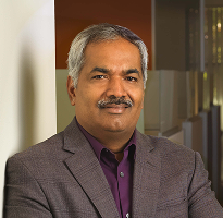 Ravi ThummarukudyCEO of Mobiveil, Inc.ShareRelated Content
 GlobalLogic26 March 2026
 GlobalLogic25 March 2026View All Insights
 GlobalLogic24 March 2026
Let's start engineering impact together
GlobalLogic provides unique experience and expertise at the intersection of data, design, and engineering.
Get in touchIn 2024, PwC Consulting and Mobiveil, a GlobalLogic company, entered into a partnership agreement to leverage their combined business capabilities and resources in the semiconductor sector. This initiative is part of PwC Consulting’s cross-industry initiative (XII), which takes a cross-organizational approach to create business synergy through long-term collaboration. The aim is to enhance semiconductor development, manufacturing technology, and performance, establish a stable supply system, and ultimately contribute to industry growth. Kimihiko Uchimura, Partner at PwC Consulting LLC, and Ravi Thummarukudy, CEO from Mobiveil, Inc.(A Hitachi Globallogic Company), discussed the challenges in the semiconductor sector and the value creation that this collaboration between the two companies aims to achieve.

From left: Sathish Kumar, Sales Director, GL Japan, Ravi Thummarukudy, CEO from Mobiveil (A Hitachi Globallogic Company), Kimihiko Uchimura, Partner at PwC Consulting LLC
PwC Consulting LLC
Partner
Kimihiko Uchimura
Mobiveil, Inc.(A Hitachi Globallogic Company)
CEO
Ravi Thummarukudy
Roles Supporting Growth in the Semiconductor Industry
Uchimura: At PwC Consulting, we have a strong expertise in strategy formulation for the semiconductor business. On the other hand, GlobalLogic is a leading company in digital engineering, with Mobiveil, led by CEO Ravi Thummarukudy, having a strong focus on VLSI & Hardware engineering and embedded technologies in semiconductors. The partnership agreement that combines these strengths is an exciting collaboration that will lead to dynamic business developments in the semiconductor field.
Ravi: Indeed. In 2023, Mobiveil became part of GlobalLogic, a subsidiary of Hitachi Ltd based in the United States. Our vision is to be a trusted partner for our customers in developing digital solutions from “Chips to Cloud” across many verticals. By leveraging GlobalLogic’s presence in 25 countries and its 33,500 global teammates, we can contribute significantly to many companies and the entire industry.
Uchimura: In our partnership, our role is to support the upstream semiconductor business by formulating digital business strategies, providing analyses, and advising on investment decisions. Furthermore, we can help establish new business models and support business development based on market and customer analyses.
Ravi: The specific operations and service designs beyond that point are where GlobalLogic excels. Our role is to help our customers deliver products to the market quickly, all while considering economic efficiency.
Diagram – Diagram of the roles of both companies.

Uchimura: In the midstream to downstream business, creating use cases and developing MVPs (Minimum Viable Products) are essential for establishing new business models. In this regard, GlobalLogic provides unique engineering and digital transformation services.
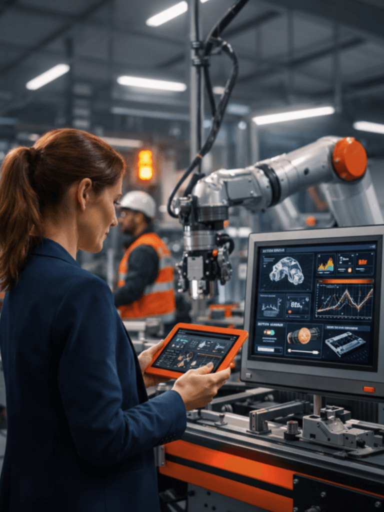
Ravi: Yes. Taking AI as an example, various companies and industries are exploring different approaches to utilizing it, but the current reality is that efforts often end at the PoC (Proof of Concept) or testing stage and do not lead to increased efficiency or productivity in operations. To address this, we have created GlobalLogic Velocity AI, a comprehensive suite of AI-powered service offerings. It’s about enabling any company to become an Intelligent Enterprise and helping them accelerate product development, improve operations, and enhance customer experiences by integrating AI, digital, and human expertise. Apart from that, Globallogic also has a unique “Lab Model” as a new framework for achieving true digital transformation (DX). This model involves providing managed services and collaboratively developing the customer’s product, whether it is hardware or software.
GlobalLogic/Mobiveil services – Complex Engineering from Chip to Cloud

Potential Challenges for Japanese Companies
Uchimura: In the domestic semiconductor market in Japan, research and development as well as mass production of next-generation semiconductors by 2030 are critical themes, with significant public support in motion, including subsidies. Among these, the mass production of advanced semiconductors in Japan is gaining attention. Currently, the smallest circuit line width that can be mass-produced is 3nm, and the national production of 2nm advanced semiconductors is planned for 2027, a technology not yet realized by companies worldwide.

Ravi Thummarukudy, CEO from Mobiveil,(A Hitachi Globallogic Company)
Ravi: Japan is incredibly attractive both technologically and as a market, having brought a variety of exciting electronics products into the world, not just semiconductors. Personally, I learned what is necessary for the semiconductor business from our Japanese customers during the semiconductor boom of the 90s when Japan was the source of semiconductors for the world. Over the past 10 years, I’ve closely observed Japanese companies move away from semiconductors and create new innovations in systems solutions. I believe Japanese companies have the ability to innovate in the semiconductor field once again in the future.
Uchimura: I hope for that as well. However, from a consulting perspective on industrial revitalization, I think there are challenges in acquiring customers. While mass production of advanced semiconductors is highly anticipated for the growth of the domestic semiconductor industry, the challenges lie in identifying “what the industry needs are” and “which application markets have customers.” In strategizing for customer acquisition, recognizing the rising demand for customized AI semiconductors is crucial, along with capturing the market needs for changing advanced semiconductors. Flexible production of small quantities in a wide variety of types is undoubtedly required, and how to capture these market needs will be key to success.
Ravi: In terms of business growth, resource shortages are also a challenge. This is an area where we can collaborate, and under the strategies devised by PwC, I believe we can support business expansion with a global resource mix blending Japan and overseas.
Diagram – Explanation of customer targets, etc.


Technological Trends in the Era of Generative AI
Uchimura: The demand for semiconductors continues to rise. However, challenges remain, such as the development of advanced technologies to meet market demands and establishment a stable supply system. The future growth of semiconductor companies will be influenced by their ability to create and deliver high-performance semiconductors promptly.
Ravi: On the supply side, the resilience of the supply chain is the primary challenge. Semiconductors have been around since the 1990s and have been commonly used as components in electronics and vehicles. At that time, the supply of semiconductors was stable, which meant their presence was largely unnoticed. However, the COVID-19 pandemic drastically changed this situation. Manufacturing and distribution issues made semiconductors difficult to obtain, and their importance became strongly recognized across industries.
Uchimura: The practical application of AI and the accompanying increase in demand are factors in the semiconductor shortage. In the advancement of semiconductors powering generative AI, new technologies like chiplets have recently emerged. Conventional semiconductor chips have been miniaturized to enhance the 2D (flat) integration density, but the limits of miniaturization are approaching. Chiplets, which stack or combine semiconductor chips vertically in 2.5D & 3D layers, are gaining attention. As the sophistication of generative AI utilization progresses, it is believed that the chiplet market will significantly grow.

Balancing Standardization and Customization
Uchimura: I believe the keywords in the future semiconductor market will be robotics and AI. In this context, we need to consider the standardization and customization of semiconductors. There is a demand for product development featuring high performance, low power, and low cost for semiconductors to be installed in robots that perform various functions, thereby pursuing competitive advantage. In other words, there is a need for small-lot, multi-variety production of advanced semiconductors, with anticipated growth in the application market driven by robotics and AI.
Ravi: Customization requires designing semiconductor chips for specific applications or systems. Emerging application markets include sectors such as Edge AI, healthcare, and military, where semiconductor chips must meet needs in small lots ranging from around 1,000 to 100,000 units. I believe there are three key themes in this effort: miniaturization, performance enhancement, and AI-based development. AI has directions towards both cloud and edge, and in about 10 years, if not earlier, AI embedded systems will become commonplace, with cloud or edge, or both, being incorporated.
Uchimura: Currently, the main brain for AI utilization is in the cloud, with the common structure being to access the cloud from devices such as PCs and smartphones to obtain answers from AI. For example, smartphones upload text, images, and audio to the cloud, where AI performs analyses and returns the results to the smartphone. To change this architecture and perform the processes on the edge rather than the cloud, the AI semiconductors embedded in edge devices need to be more advanced than ever.
Ravi: Exactly. Taking cars as an example, we enter the realm known as SDV (Software-Defined Vehicles). In the coming era, cars will become like workplaces and also homes. Therefore, the security and communication in data exchange become even more critical. Since safety is paramount for cars, autonomous driving performance must also be enhanced. If, during driving, a threat is imminent and an image of an object ahead is taken and uploaded to the cloud for AI to identify, waiting for a response could lead to a collision, affecting the driver’s life. Overcoming this challenge requires embedding the intelligence in the device, making it necessary to produce highly advanced and diverse semiconductors in small lots for the varied application needs that complete processing on the edge.
Promoting Standardization through Silicon IP
Uchimura: In the context of the increasing demand for advanced AI semiconductors for edge applications, silicon IP (semiconductor IP) and EDA (Electronic Design Automation) are also important. Before the widespread use of silicon IP, full-custom design was the standard, requiring significant time and cost to design each semiconductor from scratch. However, with silicon IP, highly advanced and optimized components are available from the initial stages of semiconductor design, greatly reducing the time from design to production.

Kimihiko Uchimura, Partner at PwC Consulting LLC
Ravi: That’s right. Historically, designs took an average of 24 to 36 months, but using silicon IP has reduced this time to 12-18 months. Additionally, standard-based third-party software and IP can now be used, accelerating interoperability. This ties back to the earlier discussion on standardization and customization, as standardization is a keyword in the semiconductor business. This change has made it possible to create complex SoCs (System on Chips) quickly and easily.
Uchimura: I believe the trend of EDA vendors providing semiconductor IPs with specific functions for reuse will continue to grow. Mobiveil, as an independent IP and services vendor, has an advantage in this area.
Ravi: Yes. In this field, Mobiveil’s strength lies in its provision of silicon IPs specialized for applications such as storage, IoT, and communication; its ability to develop silicon IPs that are easily configurable and customizable; and its robust support system. Moreover, together with GlobalLogic, we offer more services, such as Firmware & BSP / BSW development, along with validation & test automation for embedded platforms as well as cutting-edge solutions for industrial digitalization, including digital tweens, manufacturing/warehouse automation, and AI-driven production
I have been involved in semiconductors, IP, and EDA for over 30 years. From my experience, I understand the importance of a system that packages designs for reuse. I look forward to continuing to support mass production for clients across various industries using silicon IP and services.
Uchimura: By confirming each other’s strengths and roles, I’m even more excited about our collaboration that will intensify moving forward. PwC Japan is committed to “building trust in society and solving important problems.” Through the semiconductor business, let’s impact society and improve people’s lives and society as a result, supporting the transformation of businesses, industries, and society together.
 How can I help you?
- Industries